


Why "Good Enough" Isn't Enough: A Deep Dive into PCB Stencil Precision
 View
View
We've all been there: your PCB design is perfect, your components are ready, but after reflow, you're met with a nightmare of solder bridges and dry joints. Often, the culprit isn't your placement—it's a stencil that failed to meet the precision your design demanded. When you're dealing with fine-pitch components, a few microns are the difference between a working prototype and a pile of scrap.
Here is a technical breakdown of why precision is the heartbeat of stencil manufacturing:
The Need for High Precision
High precision in stencil manufacturing is vital for several reasons:
- Accurate Solder Paste Deposition: Precise apertures ensure the correct amount of solder paste is deposited, which is crucial for forming reliable solder joints.
- Minimized Solder Bridging: Accurate apertures reduce the risk of solder bridging between pads, which can cause short circuits.
- Consistent Quality: High precision stencils contribute to consistent quality across multiple boards, reducing defects and rework.
Example: JLCPCB Stencil with Small Pitch Components
To illustrate the importance of high precision in stencil manufacturing, we ordered a PCB stencil from JLCPCB designed for a board with small pitch components. We will compare the desired dimensions of the stencil apertures with the actual manufactured dimensions using a digital microscope camera.

Measuring Precision with a Digital Microscope Camera
Using a digital microscope camera, we can capture high-resolution images of the stencil apertures and measure their dimensions. This allows us to verify the precision of the stencil manufacturing process.
Desired Dimensions vs. Actual Dimensions
For our example, we used a part MHPA0606RGBDT, which is a small LED with a pad size of 0.3mm x 0.3mm. Using a digital microscope camera, we will compare the desired dimensions of the stencil apertures with the actual manufactured dimensions.
Desired Dimensions:
· Pad Size: 0.3mm x 0.3mm
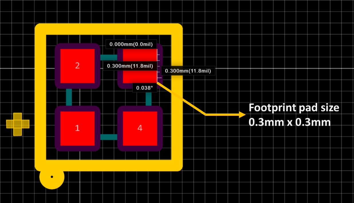
We will measure the actual dimensions of the stencil apertures for the MHPA0606RGBDT LED to ensure they match the desired specifications.
Results and Analysis
After capturing the images and measuring the apertures with the digital microscope camera, we found the following actual dimensions:
Actual Dimensions:
· Pad Size: 0.3098mm x 0.2980mm
These results show that the actual dimensions are very close to the desired dimensions, with only minor deviations. The deviations are within acceptable tolerances, demonstrating high precision in the stencil manufacturing process. This level of precision ensures accurate solder paste deposition, which is critical for the reliable performance of the assembled PCB.

🚀 Bring Your High-Density Designs to Life
At JLCPCB, we invest in the latest laser-cutting technology and inspection systems to ensure your custom designs are executed with microscopic accuracy. Whether you're working on 0201s or ultra-fine pitch ICs, we provide the precision you need to make your assembly faster and better.
- 🎁 Click to claim your $10 Stencil Coupon
- ✨ New to JLCPCB? Register now to unlock your $123 Welcome Coupon Bundle!
Sign In Or Register Comment after
No comments yet. Be the first to comment!